Electronics & Semiconductors
Empowering the Future of Microfabrication with MAXWAVE
As the electronics and semiconductor industries push the boundaries of miniaturization, performance, and reliability, the demand for ultra-precise, non-contact, and clean processing technologies has never been higher. MAXWAVE Laser offers a full suite of laser solutions—cutting, welding, marking, engraving, and cleaning—engineered to meet the exacting standards of these high-tech sectors.
Where Laser Technology Delivers the Edge
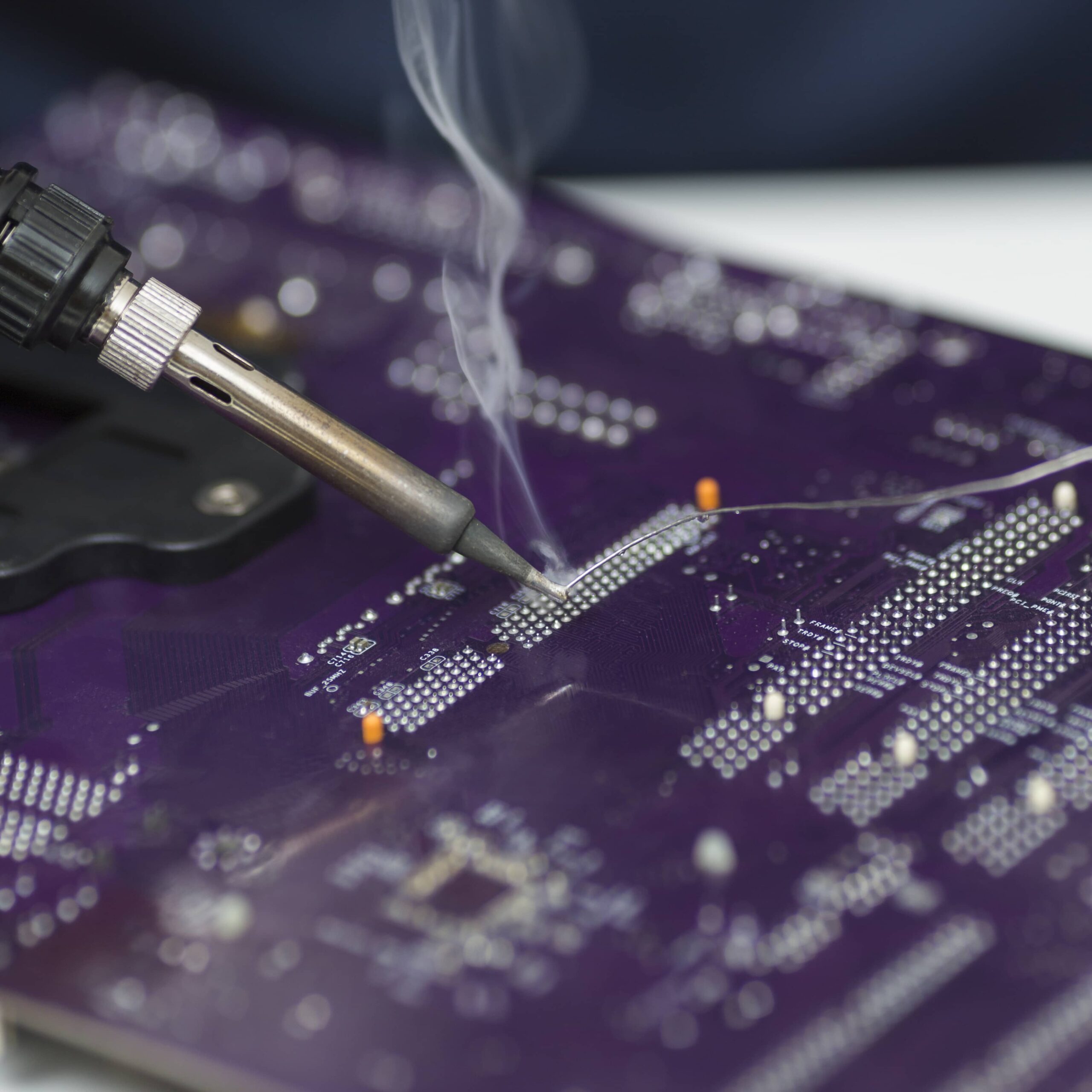
High-Precision Laser Welding
From micro-sensors to high-density interconnects, laser welding enables clean, narrow, and distortion-free joints—perfect for precision electronics manufacturing where traditional methods fall short.
- Sensor Encapsulation & Bonding
Securely welds sensor housings with minimal heat input, preserving sensitive elements. - Lithium-Ion Battery Tab Welding
Delivers high-strength welds for thin aluminum and copper tabs, ensuring conductivity and reliability in compact battery designs. - Flexible PCB Component Welding
Ideal for flex circuits and miniature connectors, providing low-stress, high-precision joints in tight layouts. - Ultra-Fine Beam Control
Non-contact process with no mechanical pressure, allowing for delicate material handling and micro-scale accuracy in confined areas.
Laser Marking for Traceability
In modern electronics manufacturing, traceability is essential for quality assurance, regulatory compliance, and anti-counterfeiting. Laser marking provides permanent, high-contrast identification on sensitive components—without damaging the substrate or requiring consumables.
Used for:
- IC chips and wafers
- Connector pins
- PCB and SMT components
- Anti-counterfeiting micro codes
- No consumables, no abrasion
- Works on metal, plastic, and ceramics
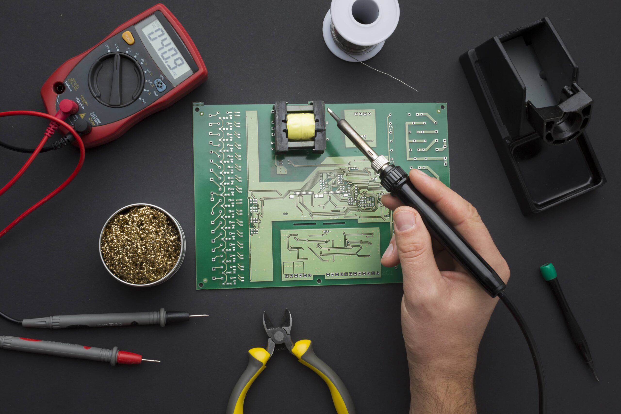
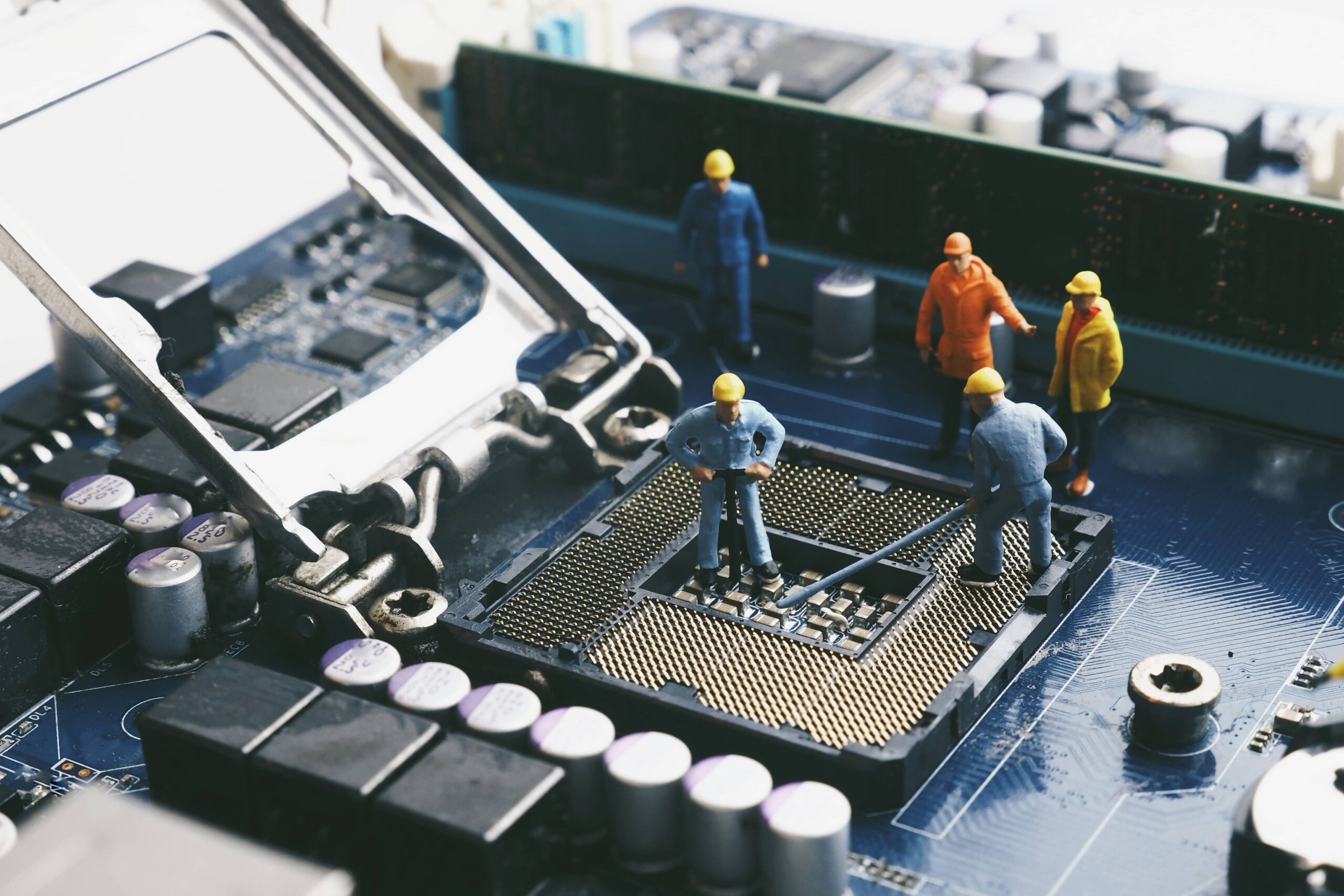
Micro-Engraving & Etching
In chip packaging, semiconductors, and advanced electronics, laser micro-engraving offers ultra-fine, low-depth precision, enabling the creation of nano-scale patterns and permanent microstructures without damaging sensitive materials.
- Die-Level ID Marking
Permanent serial numbers or wafer codes for traceability. - Package Branding
High-resolution logos or model IDs on chip packages. - Microscale Patterning
Engrave fine patterns or alignment marks on glass, ceramic, or polymer substrates. - High-Speed Precision
Rapid, contactless, high-resolution etching for miniaturized devices.
Laser Cutting - Micro Components
Our precision laser cutting systems handle flexible circuits, silicon wafers, and thin films with zero mechanical stress, making them ideal for fragile and miniaturized components.
- OLED & LCD Panel Cutting
Clean, crack-free cuts on display layers - FPC Trimming
Accurate edge shaping for flexible printed circuits - Semiconductor Die Singulation
Non-contact die separation with minimal heat impact - Protective Film Cutting
Clean contour cuts on adhesive and cover layers
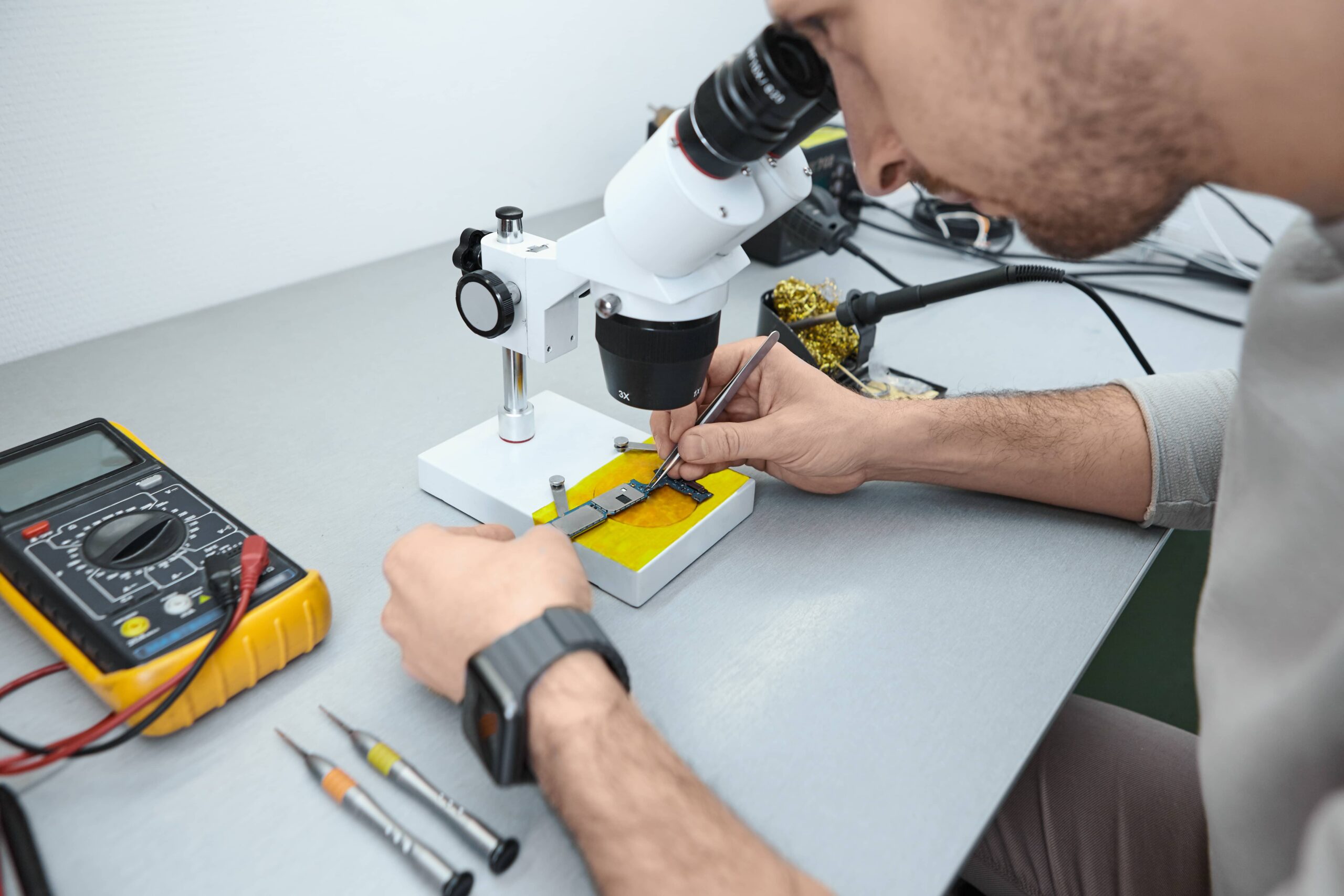
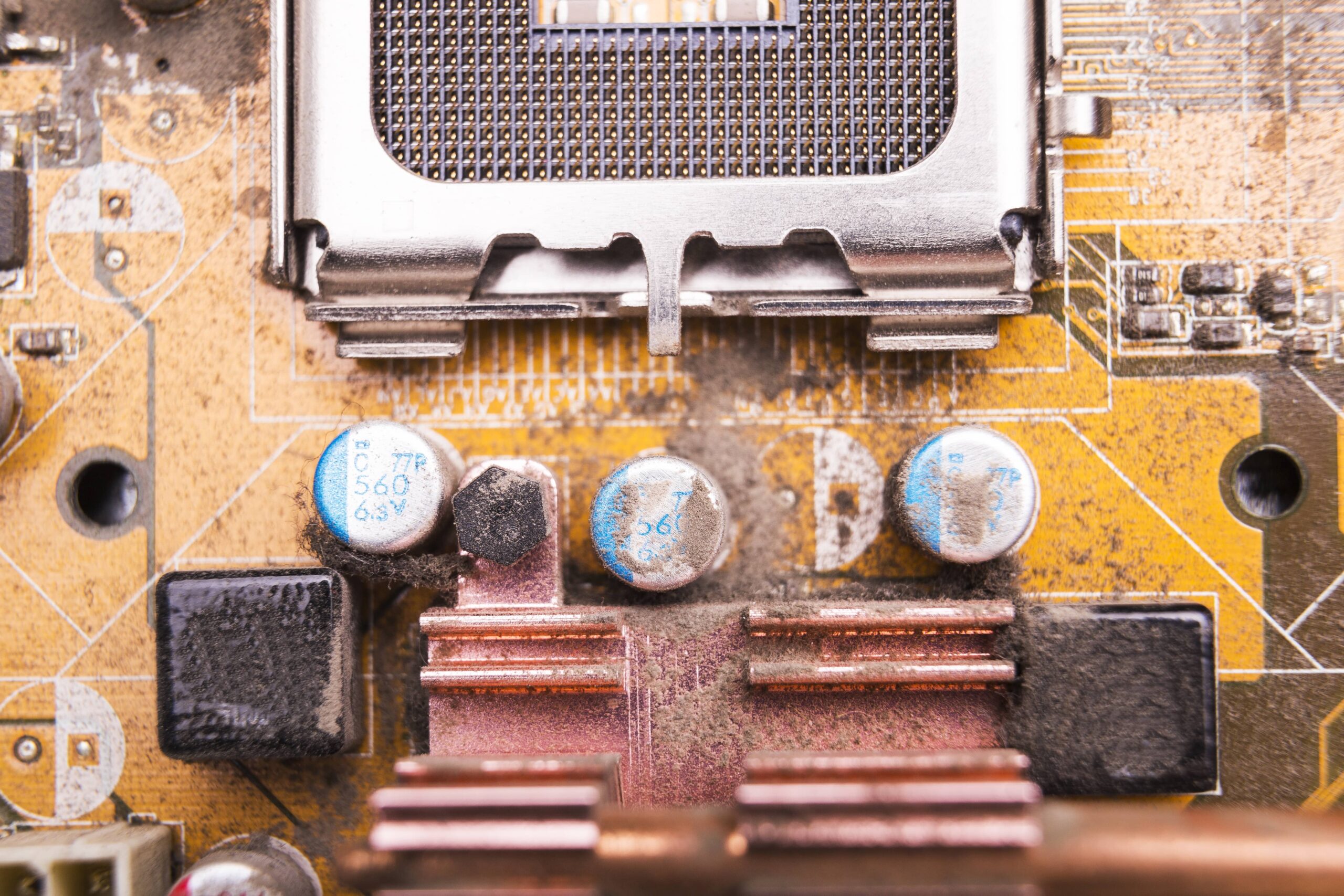
Laser Cleaning for Sensitive Parts
Laser cleaning offers a non-contact, chemical-free method to remove oxides, residues, and thin coatings from sensitive electronic components—without damaging the substrate.
- Safe for Delicate Surfaces
Ideal for PCBs, sensor housings, and semiconductor tools.
✅ laser cleaning electronics, non-abrasive cleaning - Environmentally Friendly
No solvents, no waste—green alternative to traditional cleaning.
✅ eco-friendly laser cleaning, chemical-free surface prep - High Precision & Repeatability
Controlled, programmable cleaning for pre-bonding or post-processing stages.
✅ precision laser surface treatment, repeatable cleaning process